- 您现在的位置:买卖IC网 > Sheet目录308 > ADUM6132ARWZ-RL (Analog Devices Inc)IC GATE DRIVER ISOLATED 16-SOIC
Data Sheet
ADuM6132
DIN V VDE V 0884-10 (VDE V 0884-10) INSULATION CHARACTERISTICS
The ADuM6132 is suitable for reinforced electrical isolation only within the safety limit data. Maintenance of the safety data is ensured by
protective circuits. The asterisk (*) marking on the package denotes DIN V VDE V 0884-10 approval.
Table 5.
Parameter
Test Conditions/Comments
Symbol
Value
Unit
Installation Classification per DIN VDE 0110
For Rated Mains Voltage ≤ 150 V rms
For Rated Mains Voltage ≤ 300 V rms
For Rated Mains Voltage ≤ 400 V rms
Climatic Classification
Pollution Degree (DIN VDE 0110, Table 1)
I to IV
I to III
I to II
40/105/21
2
Maximum Working Insulation Voltage
V IORM
560
V peak
Input-to-Output Test Voltage, Method B1
V IORM × 1.875 = V PR , 100% production test, t m = 1 sec,
partial discharge <5 pC
V PR
1050
V peak
Input-to-Output Test Voltage, Method A
V PR
After Environmental Tests Subgroup 1
After Input and/or Safety Test Subgroup 2
and Subgroup 3
V IORM × 1.6 = V PR , t m = 60 sec, partial discharge <5 pC
V IORM × 1.2 = V PR , t m = 60 sec, partial discharge <5 pC
896
672
V peak
V peak
Highest Allowable Overvoltage
Transient overvoltage, t TR = 10 sec
V TR
6000
V peak
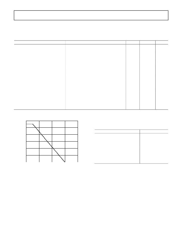
Safety-Limiting Values
Maximum value allowed in the event of a failure
(see Figure 2)
Case Temperature
Side 1 Current
T S
I S1
150
555
°C
mA
Insulation Resistance at T S
V IO = 500 V
R S
>109
?
600
500
RECOMMENDED OPERATING CONDITIONS
Table 6.
Parameter
Rating
400
300
200
100
0
Operating Temperature Range, T A
Input Supply Voltage, V DD and V DDL1
Channel A, Channel B Supply Voltage,
V DDA and V DDB1
Input Signal Rise and Fall Times
Common-Mode Transient Immunity,
Input to Output
Minimum Power-On Slew Rate (P SLEW ),
V DD and V DDL2
?40°C to +85°C
4.5 V to 5.5 V
12.5 V to 17 V
1 ms
?50 kV/μs to +50 kV/μs
1 V/ms
0
50
100
150
200
AMBIENT TEMPERATURE (°C)
Figure 2. Thermal Derating Curve, Dependence of Safety-Limiting Values
with Ambient Temperature per DIN V VDE V 0884-10
1
2
All voltages are relative to their respective ground.
The ADuM6132 power supply may fail to properly initialize if V DD and V DDL are
applied too slowly. The power supply slew rate must be faster than specified
over the entire turn-on ramp. Power-on should start from a completely
discharged state.
Rev. B | Page 5 of 16
发布紧急采购,3分钟左右您将得到回复。
相关PDF资料
ADUM6201CRIZ
ISOLATED DC-DC CONV 2CH 16SOIC
ADUM6404ARWZ
IC ISOLATOR 4CH DCDC CONV 16SOIC
ADUM7241CRZ-RL7
ISOLATOR DGTL 1KVRMS 2CH 8SOIC
ADUM7440CRQZ-RL7
IC DIGITAL ISOLATOR 4CH 16QSOP
ADUM7510BRQZ
IC DGTL ISOLATOR 5CH 16QSOP
ADZS-21364-EZLITE
KIT EVAL EZ LITE ADDS-21364
ADZS-21371-EZLITE
KIT EVAL EZLITE ADZS-21371
ADZS-21469-EZLITE
KIT EVAL EZ LITE ADSP-21469
相关代理商/技术参数
ADUM6200
制造商:AD 制造商全称:Analog Devices 功能描述:Dual-Channel, 5 kV Isolators with Integrated DC-to-DC Converter
ADUM6200ARIZ
功能描述:IC ISOLATOR DGTL 2CH 16SOIC RoHS:是 类别:隔离器 >> 数字隔离器 系列:IsoPower®, iCoupler® 产品培训模块:IsoLoop® Isolator 标准包装:50 系列:IsoLoop® 输入 - 1 侧/2 侧:5/0 通道数:5 电源电压:3 V ~ 5.5 V 电压 - 隔离:2500Vrms 数据速率:110Mbps 传输延迟:12ns 输出类型:CMOS 封装/外壳:16-SOIC(0.154",3.90mm 宽) 供应商设备封装:16-SOIC N 包装:管件 工作温度:-40°C ~ 85°C 其它名称:390-1053-5
ADUM6200ARIZ-RL
功能描述:IC ISOLATOR DGTL 2CH 16SOIC RoHS:是 类别:隔离器 >> 数字隔离器 系列:IsoPower®, iCoupler® 产品培训模块:IsoLoop® Isolator 标准包装:50 系列:IsoLoop® 输入 - 1 侧/2 侧:5/0 通道数:5 电源电压:3 V ~ 5.5 V 电压 - 隔离:2500Vrms 数据速率:110Mbps 传输延迟:12ns 输出类型:CMOS 封装/外壳:16-SOIC(0.154",3.90mm 宽) 供应商设备封装:16-SOIC N 包装:管件 工作温度:-40°C ~ 85°C 其它名称:390-1053-5
ADUM6200ARWZ
功能描述:ISOLAT DGTL 5KVRMS 2CH 16SOIC-W RoHS:是 类别:隔离器 >> 数字隔离器 系列:IsoPower®, iCoupler® 产品培训模块:IsoLoop® Isolator 标准包装:50 系列:IsoLoop® 输入 - 1 侧/2 侧:5/0 通道数:5 电源电压:3 V ~ 5.5 V 电压 - 隔离:2500Vrms 数据速率:110Mbps 传输延迟:12ns 输出类型:CMOS 封装/外壳:16-SOIC(0.154",3.90mm 宽) 供应商设备封装:16-SOIC N 包装:管件 工作温度:-40°C ~ 85°C 其它名称:390-1053-5
ADUM6200ARWZ-RL
功能描述:隔离器接口集成电路 kV 2-Ch Isolator w/ Int DC/DC Converter RoHS:否 制造商:Texas Instruments 通道数量:2 传播延迟时间: 电源电压-最大:5.5 V 电源电压-最小:3 V 电源电流:3.6 mA 功率耗散: 最大工作温度:+ 125 C 安装风格: 封装 / 箱体:SOIC-8 封装:Tube
ADUM6200CRIZ
功能描述:ISOLATED DC-DC CONV 2CH 16SOIC RoHS:是 类别:隔离器 >> 数字隔离器 系列:IsoPower®, iCoupler® 产品培训模块:IsoLoop® Isolator 标准包装:50 系列:IsoLoop® 输入 - 1 侧/2 侧:5/0 通道数:5 电源电压:3 V ~ 5.5 V 电压 - 隔离:2500Vrms 数据速率:110Mbps 传输延迟:12ns 输出类型:CMOS 封装/外壳:16-SOIC(0.154",3.90mm 宽) 供应商设备封装:16-SOIC N 包装:管件 工作温度:-40°C ~ 85°C 其它名称:390-1053-5
ADUM6200CRIZ-RL
功能描述:IC ISOLATOR DGTL 2CH 16SOIC RoHS:是 类别:隔离器 >> 数字隔离器 系列:IsoPower®, iCoupler® 产品培训模块:IsoLoop® Isolator 标准包装:50 系列:IsoLoop® 输入 - 1 侧/2 侧:5/0 通道数:5 电源电压:3 V ~ 5.5 V 电压 - 隔离:2500Vrms 数据速率:110Mbps 传输延迟:12ns 输出类型:CMOS 封装/外壳:16-SOIC(0.154",3.90mm 宽) 供应商设备封装:16-SOIC N 包装:管件 工作温度:-40°C ~ 85°C 其它名称:390-1053-5
ADUM6200CRWZ
功能描述:ISOLAT DGTL 5KVRMS 2CH 16SOIC-W RoHS:是 类别:隔离器 >> 数字隔离器 系列:IsoPower®, iCoupler® 产品培训模块:IsoLoop® Isolator 标准包装:50 系列:IsoLoop® 输入 - 1 侧/2 侧:5/0 通道数:5 电源电压:3 V ~ 5.5 V 电压 - 隔离:2500Vrms 数据速率:110Mbps 传输延迟:12ns 输出类型:CMOS 封装/外壳:16-SOIC(0.154",3.90mm 宽) 供应商设备封装:16-SOIC N 包装:管件 工作温度:-40°C ~ 85°C 其它名称:390-1053-5
